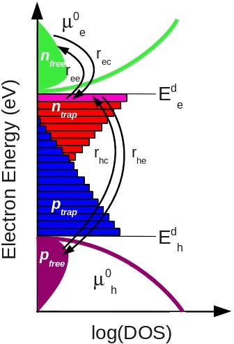
 Figure 2: A 0D energy slice through the model. |
Update 18/10/2022: Gpvdm now has a ⭐new name⭐, it is now called OghmaNano. Please go to https://www.oghma-nano.com to get the latest version of the software and documentation.
It is hoped that this new name will be easier to say and remember. For a history of OghmaNano/gpvdm click here.
You should be automatically redirected in 7 seconds.
Gpvdm's electrical model is a 1D/2D drift-diffusion model (like many others) however the special thing about gpvdm which makes it very good for disordered materials (Think organics, perovskites and a-Si) is that it goes to the trouble of explicitly solving the Shockley-Read-Hall equations as a function of energy and position space. This enables one to model effects such as mobility/recombination rates changing as a function of carrier population and enables one to correctly model transients as one does not have to assume all the carriers in the trap states have reached equilibrium. Things such as ToF transients, CELIV transients etc.. can be modeled with ease. An example of this can be seen in figure 1. Of course can be used for more ordered materials as well, you then just need to turn the traps off.
The conduction band/valance band (or LUMO/HOMO in organic semiconductor speak) are defined as
$$E_{LUMO}=-\chi-q\phi$$ $$E_{HOMO}=-\chi-E_g-q\phi$$To obtain the internal potential distribution within the device Poisson's equation is solved,
$$\nabla \cdot \epsilon_0 \epsilon_r \nabla = q (n_{f}+n_{t}-p_{f}-p_{t}-N_{ad}+-N_{ion}+a)$$where \(n_{f}\), \(n_{t}\) are the carrier densities of free and trapped electrons; \(p_{f}\) and \(p_{t}\) are the carrier densities of the free and trapped holes; and \(N_{ad}\) is the doping density. \(N_{ion}\) is the background density of perovskite ions and a is the density of mobilie ions
For free carriers the model can either use Maxwell-Boltzmann statistics i.e.
$$n_{l}=N_c exp \left (\frac{F_n-E_{c}}{kT} \right)$$and
$$p_{l}=N_v exp \left(\frac{E_{v}-F_p}{kT} \right)$$or full Fermi-dirac statistics i.e.
$$n_{free}(E_{f},T)=\int^{\infty}_{E_{min}} \rho(E) f(E,E_{f},T) dE$$and
$$p_{free}(E_{f},T)=\int^{\infty}_{E_{min}} \rho(E) f(E,E_{f},T) dE$$.where
$$f(E)=\frac{1}{1+e^{{E-E_f}/kT}}$$When using FD statistics free carriers are assumed to move in a parabolic band i.e.
$$\rho(E)_{3D}=\frac{\sqrt{E}}{4\pi^2} \left ( \frac{2m^{*}}{\hbar^2}\right )^{3/2}$$The average energy of the carrier distribution is given as:
$$\bar{W}(E_{f},T)=\frac{\int^{\infty}_{E_{min}} E \rho(E) f(E,E_{f},T) dE}{\int^{\infty}_{E_{min}} \rho(E) f(E,E_{f},T) dE}$$
 Figure 2: A 0D energy slice through the model. |
To describe charge becoming trapping into trap states and recombination associated with those states the model uses Shockley-Read-Hall (SRH) theory. A 0D depiction of this SRH recombination and trapping is shown in figure 2. The free electron and hole carrier distributions are labeled as \(n_{free}\) and \(p_{free}\) respectively. The trapped carrier populations are denoted with \(n_{trap}\) and \(p_{trap}\), they are depicted with filled red and blue boxes. SRH theory describes the rates at which electrons and holes become captured and escape from the carrier traps. If one considers a single electron trap, the change in population of this trap can be described by four carrier capture and escape rates as depicted in figure 2. The rate \(r_{ec}\) describes the rate at which electrons become captured into the electron trap, \(r_{ee}\) is the rate which electrons can escape from the trap back to the free electron population, \(r_{hc}\) is the rate at which free holes get trapped and \(r_{he}\) is the rate at which holes escape back to the free hole population. Recombination is described by holes becoming captured into electron space slice through our 1D traps. Analogous processes are also defined for the hole traps.
For each trap level the carrier balance
$$\frac{\delta n_t}{\partial t}=r_{ec}-r_{ee}-r_{hc}+r_{he}$$is solved, giving each trap level an independent quasi-Fermi level. Each point in position space can be allocated between 10 and 160 independent trap states. The rates of each process \(r_{ec}\), \(r_{ee}\), \(r_{hc}\), and \(r_{he}\) are give in table 1 below. The escape probabilities are given by:
$$e_n=v_{th}\sigma_{n} N_{c} exp \left ( \frac{E_t-E_c}{kT}\right )$$and
$$e_p=v_{th}\sigma_{p} N_{v} exp \left ( \frac{E_v-E_t}{kT}\right )$$where \(\sigma_{n,p}\) are the trap cross sections, \(v_{th}\) is the thermal emission velocity of the carriers, and \(N_{c,v}\) are the effective density of states for free electrons or holes. The distribution of trapped states (DoS) is defined between the mobility edges as
$$\rho^{e/h}(E)=N^{e/h}exp(E/E_{u}^{e/h})$$
Table 1: SRH capture escape rates |
where, \(N_{e/h}\) is the density of trap states at the LUMO or HOMO band edge in states/eV and where \(E_{U}^{e/h}\) is slope energy of the density of states. The value of \(N_{t}\) for any given trap level is calculated by averaging the DoS function over the energy (\(\Delta E\) ) which a trap occupies:
$$N_{t}(E)=\frac{\int^{E+\Delta E/2}_{E-\Delta E/2} \rho^{e}{E} dE}{\Delta E}$$The occupation function is given by the equation,
$$f(E_{t},F_{t})=\frac{1}{e^{\frac{E_{t}-F_{t}}{kT}}+1}$$Where, \(E_{t}\) is the trap level, and \(F_{t}\) is the Fermi-Level of the trap. The carrier escape rates for electrons and holes are given in table 1.
Free-to-free recombination is described using equation
$$R_{free}=k_{r}(n_{f}p_{f}-n_{0}p_{0})$$Auger recombination is included in the model as
$$R^{AU}=(C^{AU}_{n}n+C^{AU}_{p}p)(np-n_{0}p_{0})$$where \(C^{AU}_{n}\) and \(C^{AU}_{p}\) are the Auger coefficient of electrons and holes in \(m^6 s^{-1}\). This can be set in the electrical paramter editor.
To describe charge carrier transport, the bi-polar drift-diffusion equations are solved in position space for electrons,
$$\boldsymbol{J_n} = q \mu_e n_{f} {\nabla E_{c}} + q D_n {\nabla n_{f}}$$and holes,
$$\boldsymbol{J_p} = q \mu_h p_{f} {\nabla E_{v}} - q D_p {\nabla p_{f}}$$Conservation of charge carriers is forced by solving the charge carrier continuity equations for both electrons,
$$\nabla \boldsymbol{J_n} = q (R-G+\frac{\partial n}{\partial t})$$and holes
$$\nabla \boldsymbol{J_p} = - q (R-G+\frac{\partial p}{\partial t})$$where \(R\) and \(G\) are the net recombination and generation rates per unit volume respectively.
There are three optical model available:
1. A model which assumes the distributions of photons in the device is flat and uniform.
2. A model which assumes light intensity decays exponentially as it penetrates the device.
3. A standard transfer matrix approach where the forward and backward propagating waves are solved, taking into account reflections at interfaces.
The full description of the model can be found in this paper.